A�
� R�
� C�
� H�
� I�
� V�
� E�
� I�
� N�
� F�
� O�
� R�
� M�
� A�
� T�
� I�
� O�
� N�
� A�
� R�
� C�
� H�
� I�
� V�
� E�
� I�
� N�
� F�
� O�
� R�
� M�
� A�
� T�
� I�
� O�
� N�
� MRF21010LR1 MRF21010LSR1�
� 3�
� RF Device Data�
� Freescale Semiconductor�
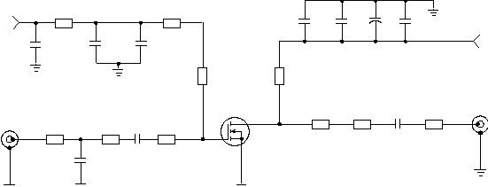
� Figure 1. MRF21010L Test Circuit Schematic�
� RF�
� INPUT�
� RF�
� OUTPUT�
� Z1�
� VGG�
� C2�
� C10�
� C3�
� +�
� DUT�
� VDD�
� Z6 0.453″�
� x 1.118″�
� Microstrip�
� Z7 0.921″�
� x 0.154″�
� Microstrip�
� Z8 0.925″�
� x 0.087″�
� Microstrip�
� PCB Taconic TLX8--0300, 0.030″,�
� εr�
� = 2.55�
� Z2�
� C8�
� C7�
� Z6�
� Z7�
� C6�
� Z4�
� R2�
� C4�
� C1�
� Z3�
� Z8�
� +�
� C9�
� +�
� R1�
� C5�
� Z5�
� Z1 0.964″�
� x 0.087″�
� Microstrip�
� Z2 0.905″�
� x 0.087″�
� Microstrip�
� Z3 0.433″�
� x 0.512″�
� Microstrip�
� Z4 1.068″�
� x 0.087″�
� Microstrip�
� Z5 0.752″�
� x 0.087″�
� Microstrip�
� Table 5. MRF21010L Test Circuit Component Designations and�
� Values�
� Part�
� Description�
� Part Number�
� Manufacturer�
� C1 * (eared)�
� 2.2 pF Chip Capacitor�
� 100B2R2BW�
� ATC�
� (earless)�
� 1.8 pF Chip Capacitor�
� 100B1R8BW�
� ATC�
� C2�
� 0.5 pF Chip Capacitor�
� 100B0R5BW�
� ATC�
� C3, C9�
� 10�
� μF, 35 V Tantalum Chip Capacitors�
� 293D106X9035D2T�
� Sprague--Vishay�
� C4, C7�
� 1 nF Chip Capacitors�
� 100B102JW�
� ATC�
� C5, C6�
� 5.6 pF Chip Capacitors�
� 100B5R6BW�
� ATC�
� C8�
� 470�
� μF, 63 V Electrolytic Capacitor�
� C10�
� 10 pF Chip Capacitor�
� 100B100GW�
� ATC�
� N1, N2�
� Type N Connector Flange Mounts�
� 3052--1648--10�
� Macom�
� R1�
� 1.0 k?�
� Chip Resistor (0805)�
� R2�
� 12�
� ?�
� Chip Resistor (0805)�
� * Piece part depending on eared / earless version of the device.�
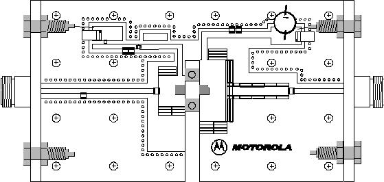
� Figure 2. MRF21010L Test Circuit Component Layout�
� RF Output�
� C2�
� C1�
� C3�
� C4 C5�
� R1�
� R2�
� C6 C7�
� C8�
� C9�
� C10�
� CUTOUT AREA�
� VGG�
� VDD�
� RF Input�
� C--XM--00--001--01�
� MRF21010�
� Freescale has begun the transition of marking Printed Circuit Boards (PCBs) with the Freescale Semiconductor�
� signature/logo. PCBs may have either Motorola or Freescale�
� markings during the transition period. These changes�
� will have no impact on form, fit or function of the current product.�
�  �
�
� � �  �
�
� � �  �
�
� � �  �
�
� � �  �
�
� �  �
�
� �  �
�
� � �  �
�
� �  �
�
� � �  �
�
� � �  �
�
� � 发布紧急采购,3分钟左右您将得到回复。
相关PDF资料
MRF21030LR3
IC MOSFET RF N-CHAN NI-400
MRF21045LR5
IC MOSFET RF N-CHAN NI-400
MRF21085LSR3
IC MOSFET RF N-CHAN NI-780S
MRF281ZR1
IC MOSFET RF N-CHAN NI-200Z
MRF282SR1
IC MOSFET RF N-CHAN NI-200S
MRF372R3
IC MOSFET RF N-CHAN NI-860C3
MRF373ALSR5
MOSFET RF N-CHAN 32V 75W NI-360S
MRF374A
IC MOSFET RF N-CHAN NI-650
相关代理商/技术参数
MRF21010LSR5
功能描述:IC MOSFET RF N-CHAN NI-360S RoHS:是 类别:分离式半导体产品 >> RF FET 系列:- 产品目录绘图:MOSFET SOT-23-3 Pkg 标准包装:3,000 系列:- 晶体管类型:N 通道 JFET 频率:- 增益:- 电压 - 测试:- 额定电流:30mA 噪音数据:- 电流 - 测试:- 功率 - 输出:- 电压 - 额定:25V 封装/外壳:TO-236-3,SC-59,SOT-23-3 供应商设备封装:SOT-23-3(TO-236) 包装:带卷 (TR) 产品目录页面:1558 (CN2011-ZH PDF) 其它名称:MMBFJ309LT1GOSMMBFJ309LT1GOS-NDMMBFJ309LT1GOSTR
MRF21030D
制造商:MOTOROLA 制造商全称:Motorola, Inc 功能描述:RF POWER FIELD EFFECT TRANSISTORS N-CHANNEL ENANCEMENT- MODE LATERAL MOSFETS
MRF21030LR3
功能描述:射频MOSFET电源晶体管 30W 2.2GHZ LDMOS NI400L RoHS:否 制造商:Freescale Semiconductor 配置:Single 晶体管极性: 频率:1800 MHz to 2000 MHz 增益:27 dB 输出功率:100 W 汲极/源极击穿电压: 漏极连续电流: 闸/源击穿电压: 最大工作温度: 封装 / 箱体:NI-780-4 封装:Tray
MRF21030LR5
功能描述:IC MOSFET RF N-CHAN NI-400 RoHS:是 类别:分离式半导体产品 >> RF FET 系列:- 产品目录绘图:MOSFET SOT-23-3 Pkg 标准包装:3,000 系列:- 晶体管类型:N 通道 JFET 频率:- 增益:- 电压 - 测试:- 额定电流:30mA 噪音数据:- 电流 - 测试:- 功率 - 输出:- 电压 - 额定:25V 封装/外壳:TO-236-3,SC-59,SOT-23-3 供应商设备封装:SOT-23-3(TO-236) 包装:带卷 (TR) 产品目录页面:1558 (CN2011-ZH PDF) 其它名称:MMBFJ309LT1GOSMMBFJ309LT1GOS-NDMMBFJ309LT1GOSTR
MRF21030LSR3
制造商:FREESCALE 制造商全称:Freescale Semiconductor, Inc 功能描述:RF Power Field Effect Transistors N-Channel Enhancement-Mode Lateral MOSFETs
MRF21030R3
制造商:MOTOROLA 制造商全称:Motorola, Inc 功能描述:RF POWER FIELD EFFECT TRANSISTORS N-CHANNEL ENANCEMENT- MODE LATERAL MOSFETS
MRF21030S
制造商:Motorola Inc 功能描述:MOSFET Transistor, N-Channel, SOT-391B
MRF21030SR3
制造商:MOTOROLA 制造商全称:Motorola, Inc 功能描述:RF POWER FIELD EFFECT TRANSISTORS N-CHANNEL ENANCEMENT- MODE LATERAL MOSFETS